Purpose
The RT2568 is a sink/source tracking termination regulator. This document explains the function and use of the RT2568 evaluation board (EVB), and provides information to enable operation, modification of the evaluation board and circuit to suit individual requirements.
Introduction
General Product Information
The RT2568 is a sink/source tracking termination regulator. It is specifically designed for low-cost and low-external component count systems. The RT2568 possesses a high speed operating amplifier that provides fast load transient response and only requires a minimum 10μF x 3 ceramic output capacitor. The RT2568 supports remote sensing functions and all features required to power the DDRIII and Low Power DDRIII/DDRIV VTT bus termination according to the JEDEC specification. In addition, the RT2568 provides an open-drain PGOOD signal to monitor the output regulation and an EN signal that can be used to discharge VTT during S3 (suspend to RAM) for DDR applications. The RT2568 is available in the thermal efficient package, WDFN-10L 3x3.
Product Feature
-
VIN Input Voltage Range : 1.1V to 3.5V
-
VCNTL Input Voltage Range : 2.9V to 5.5V
-
Support Ceramic Capacitors
-
Power Good Indicator
-
10mA Source/Sink Reference Output
-
Meet DDRI, DDRII JEDEC Spec
-
Support DDRIII, Low Power DDRIII/DDRIV VTT Applications
-
Soft-Start Function
-
UVLO and OCP Protection
-
Thermal Shutdown
Applications
-
Notebook/Desktop/Server
-
Telecom/Datacom, GSM Base Station, LCD-TV/PDPTV, Copier/Printer, Set-Top Box
Key Performance Summary Table
|
Key Features
|
Evaluation Board Number : PCB027_V1
|
|
Input Voltage Range
|
1.1V to 3.5V
|
|
VCNTL Input Voltage Range
|
2.9V to 5.5V
|
|
Max Output Current
|
3A
|
|
Default Output Voltage
|
Set by REFIN pin voltage level (VOUT = VREFIN)
|
|
Default Marking & Package Type
|
RT2568GQW, WDFN-10L 3x3
|
Bench Test Setup Conditions
Headers Description and Placement
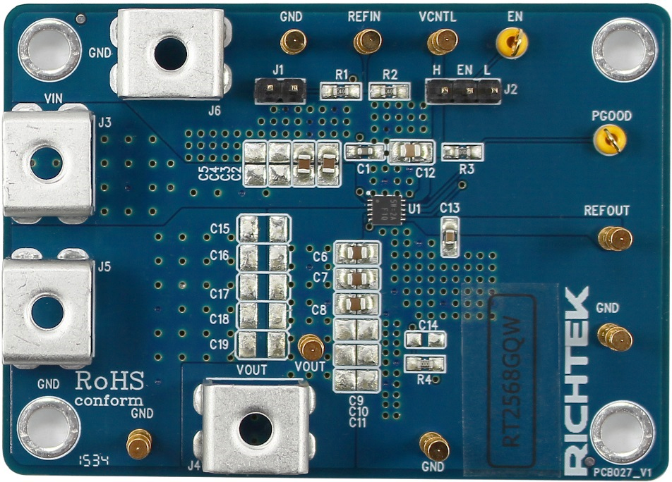
Please carefully inspect the EVB IC and external components, comparing them to the following Bill of Materials, to ensure that all components are installed and undamaged. If any components are missing or damaged during transportation, please contact the distributor or send e-mail to evb_service@richtek.com
Test Points
The EVB is provided with the test points and pin names listed in the table below.
|
Test point/
Pin name
|
Signal
|
Comment (expected waveforms or voltage levels on test points)
|
|
VIN
|
Input voltage
|
Input voltage range = 2.9V to 5.5V
|
|
VOUT
|
Output voltage
|
Power output of the regulator.
|
|
EN
|
Enable test point
|
Enable Control Input. EN = High (higher than 1.7V) for ON operation, while EN = Low (lower than 0.3V) for OFF operation.
|
|
GND
|
Ground
|
Ground.
|
|
VCNTL
|
Control voltage input
|
Control voltage input. Connect this pin to the 3.3V or 5V power supply. A ceramic decoupling capacitor with a value 4.7µF is required.
|
|
REFIN
|
Reference input
|
Reference input.
|
|
REFOUT
|
Reference output
|
Reference output. Connect to GND through a 0.1µF ceramic capacitor.
|
|
PGOOD
|
Power good output test point
|
Power good open-drain output. Connect a pull-up resistor between this pin and VCNTL pin.
|
Power-up & Measurement Procedure
1. Short J1 and the (1, 2) pin of J2 by jumper respectively.
2. Provide input voltage (2.9V < VCNTL < 5.5V) to VCNTL pin.
3. Connect input power (1.1V < VIN < 3.5V) and input ground to Vin and GND pins respectively.
4. Connect positive end and negative end of load to Vout and GND of output pins respectively.
5. The output voltage of (VOUT) can be set by R1 and R2 :

6. If J1 is not shorted by Jumper, the output voltage can be set by the input voltage of REFIN pin :
VOUT = VREFIN
Specification
|
Parameter
|
Symbol
|
Min
|
Typ.
|
Max
|
Units
|
|
Control Input Voltage
|
VCNTL
|
2.9
|
|
5.5
|
V
|
|
Supply Input Voltage
|
VIN
|
1.1
|
|
3.5
|
V
|
|
VOUT Source Current Limit
|
ILIM_VOUT_SR
|
3.5
|
|
5.5
|
A
|
|
VOUT Sink Current Limit
|
ILIM_VOUT_SK
|
3.5
|
|
5.5
|
A
|
|
REFIN Voltage Range
|
VREFIN
|
0.5
|
|
1.8
|
V
|
Schematic, Bill of Materials & Board Layout
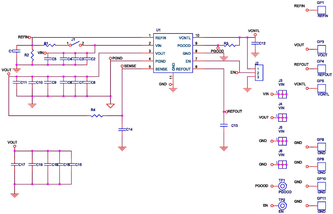
EVB Schematic Diagram
Bill of Materials
|
Reference
|
Qty
|
Part Number
|
Description
|
Package
|
Manufacture
|
|
U1
|
1
|
RT2568GQW
|
DDR Termination Regulator
|
WDFN-10L 3x3
|
RICHTEK
|
|
C2, C3, C6, C7, C8
|
5
|
GRM219R61A106KE44D
|
10µF/X5R/16V
|
C-0805
|
MURATA
|
|
C13
|
1
|
C1608X7R1H104K080AA
|
0.1µF/50V/X7R
|
C-0603
|
TDK
|
|
C12
|
1
|
C2012X5R0J475KT00HW
|
4.7µF/X5R/6.3V
|
C-0805
|
TDK
|
|
C1
|
1
|
0603B102K500
|
1nF/50V/X7R
|
C-0603
|
WALSIN
|
|
C4, C5, C9, C10, C11, C14, C15, C16, C17, C18, C19
|
11
|
|
NC
|
|
|
|
R1, R2
|
2
|
|
10k
|
R-0603
|
|
|
R3
|
1
|
|
100k
|
R-0603
|
|
|
R4
|
1
|
|
0
|
|
|
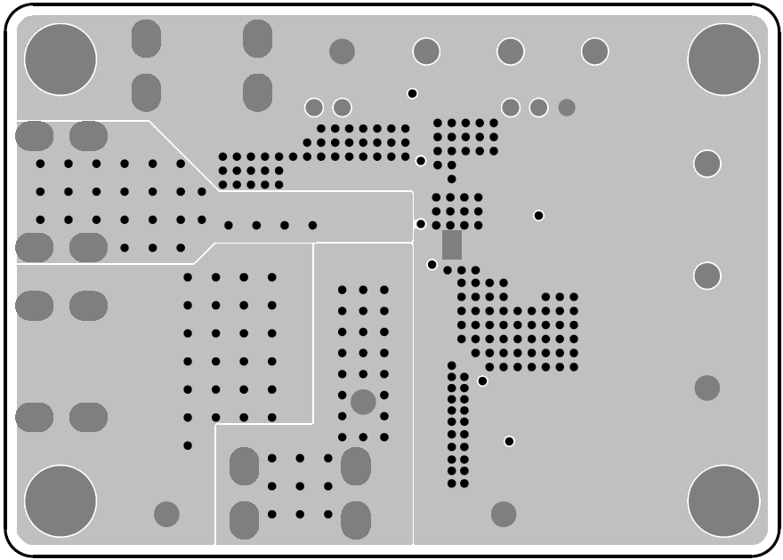
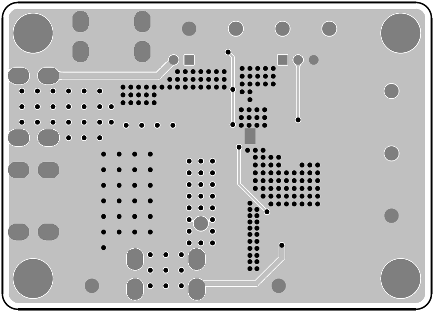
PCB Layout
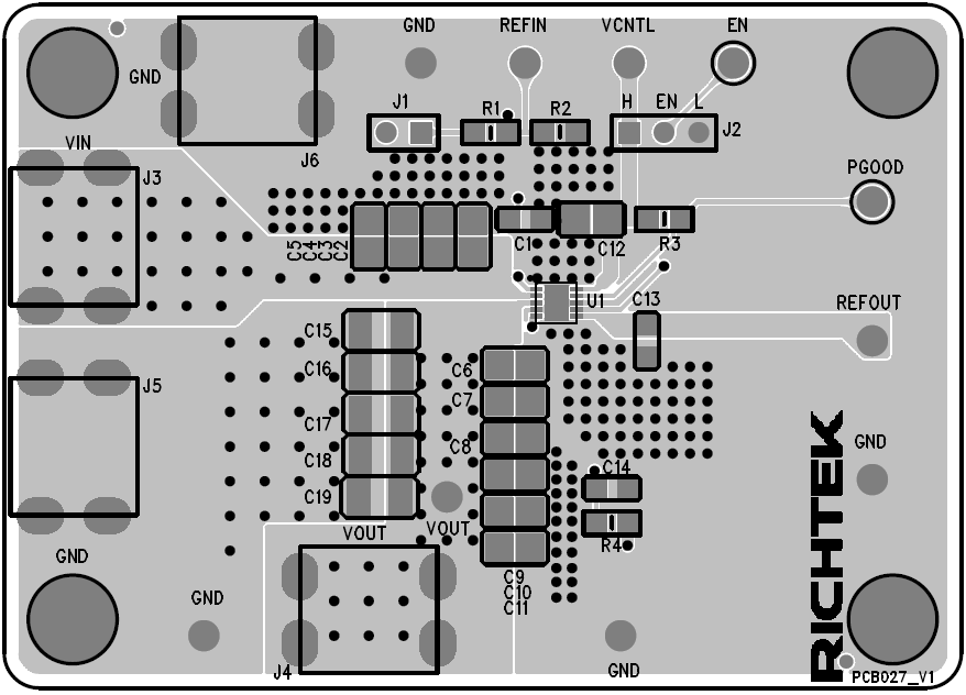
Top View (1st layer)
PCB Layout—Inner Side (2nd Layer)
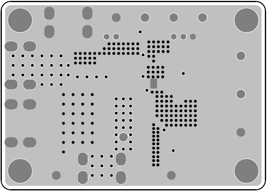
PCB Layout—Inner Side (3rd Layer)
Bottom View (4th Layer)